
DIP vs SMD vs COB vs IMD: A Complete Guide to LED Display Packaging Technologies
- LEKLED
- Apr 8
- 3 min read
Updated: Apr 9
Overview of LED Display Packaging Technologies
As a key component of modern information displays, the performance of LED screens largely depends on the advancement of LED packaging technologies. With continuous improvements in display technology and increasing application demands, LED packaging has evolved from traditional Through-Hole (DIP) to Surface-Mounted (SMD) and, more recently, to Integrated Packaging technologies like COB and IMD. This article provides a comparative overview of these three major packaging types.
1. Through-Hole Packaging (DIP)
Through-hole packaging was the dominant LED packaging method from the 1970s until around 2010. It features a PN junction semiconductor placed onto a lead frame, encapsulated with an epoxy resin dome.
Structural Features: The LED chip is mounted on metal leads and covered with a dome-shaped epoxy resin.
Optical Characteristics: Non-directional light emission, suitable for wide viewing angles due to the round lens design.
Thermal Management: 90% of the heat is dissipated through the metal pins into the PCB.
Applications: Widely used in early outdoor LED displays with pixel pitches of P10mm or larger.
Disadvantages: Bulky size, limited brightness, complex assembly process; gradually being phased out.
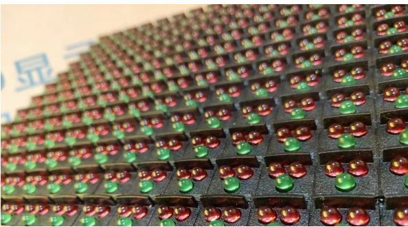
2. Surface-Mounted Packaging (SMD)

With technological advancements, SMD (Surface-Mounted Device) packaging has become mainstream. Tiny LED chips are mounted directly onto the PCB using automated machinery, allowing for compact and high-density designs.
Structural Features: LEDs are cube-shaped and surface-mounted directly on the PCB.
Optical Characteristics: Single-directional, front-facing emission with uniform brightness.
Advantages:
Compact size and lightweight;
Suitable for high-density displays;
Ideal for P1.0mm to P10mm pixel pitch displays;
Excellent color consistency and image clarity.
Disadvantages: Not suitable for ultra-fine pitch displays (< P1.0mm) due to limitations in precision and reliability.
3. Integrated Packaging (COB & IMD)

To overcome the limitations of SMD in fine-pitch applications, integrated packaging technologies have emerged, primarily COB (Chip On Board) and IMD (Integrated Matrix Devices).
COB Packaging (Chip On Board)
COB technology mounts multiple LED chips directly onto the PCB, eliminating the need for traditional surface mounting steps.
Advantages:
Simplified structure and improved reliability;
Strong impact resistance;
Lower thermal resistance and better heat dissipation.
Disadvantages:
Lower production yield;
Inconsistent uniformity;
Requires calibration before leaving the factory.
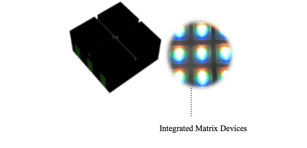
IMD Packaging (Integrated Matrix Devices)
IMD packaging integrates multiple pixel units into a single module, combining the strengths of both SMD and COB.
Advantages:
High precision and excellent consistency;
Better color uniformity than COB and higher yield than SMD;
Suitable for mass production and industrial-scale applications;
Commonly used in 4-in-1 modules.
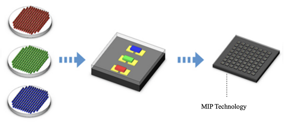
MIP Packaging (Micro LED in Package)
To address the yield and cost challenges of full-panel Micro LED manufacturing, MIP (Micro LED in Package) has emerged as a new-generation packaging architecture. MIP represents a hybrid solution that combines Micro LED chips with discrete packaging techniques, segmenting large display panels into smaller, independently packaged units.
This modular approach allows for better yield control on small-area substrates and shifts the testing process from the chip fabrication stage to the packaging stage—greatly improving production efficiency and reducing costs.
Advantages:
Higher yield rates due to smaller unit packaging and localized defect control;
Reduced cost and faster production by moving testing from chip to packaging stage;
Flexible and scalable for mass production of Micro LED displays;
Better repairability and modular replacement capability.
Disadvantages:
Complex integration of Micro LED chips and driving circuitry;
More intricate manufacturing process compared to traditional SMD;
Still evolving, with limited standardization across the industry.
MIP is considered a promising solution for next-generation ultra-fine-pitch displays, especially in applications such as AR/VR, wearable devices, automotive displays, and high-end consumer electronics.
Comparison Summary
Packaging Type | Optical Characteristics | Thermal Management | Application Range | Advantages | Disadvantages |
DIP | Non-directional emission | Heat dissipation through pins | Outdoor displays (>P10mm) | Simple structure, reliable | Bulky, low brightness, outdated |
SMD | Front-facing, uniform light | Via solder pads on PCB | P1.0mm–P10mm | Compact, high density, good image quality | Not suitable for <P1.0mm |
COB | Uniform surface emission | Excellent thermal performance | Small pitch, high-protection screens | High reliability, impact resistant | Low yield, poor consistency |
IMD | High brightness and consistency | Good heat dissipation | Fine-pitch LED displays | High precision, scalable for mass production | Higher cost |
Conclusion
As LED display technology continues to evolve toward higher resolution and smaller pixel pitch, packaging technologies are also advancing. COB and IMD are increasingly seen as the next-generation solutions, gradually replacing older packaging methods. Their advantages in precision, reliability, and efficiency make them well suited for modern high-performance LED displays.
Kommentare